[ASICs] [Chip Typen] [Chip Aufbau] [Entwicklung] [Schnittstellen] [Glossar]
[Buffer Types] [Interfaces] [Networks] [IEEE 802 Networks] [Data Lines] [Protocols] [Organazations]
 Buffer Types
The following page gives a rough overview about several buffer types in terms of employment, electrical signal specification, possible data rates and other characteristics. Not every description holds the complete set of parameters and my intention is not to summarize the signal specification. Depending upon what I´m going to find in the internet the descriptions will be completed.
Buffer Type Overview
Fail-safe Buffer
AGP-2X Advanced Graphics Port
CML Current Mode Logic
CMOS Complementary Metal Oxide Semiconductor
CTT Center Tap Terminated
ECL Emitter Coupled Logic
PECL Positive Referenced Emitter Coupled Logic
GTL Gunning Transceiver Logic Terminated
GTL+ Gunning Transceiver Logic Plus
HSTL High-Speed Transceiver Logic
SSTL Stub Series Terminated Logic (SSTL2 / SSTL3)
LVCMOS Low Voltage CMOS
LVDS Low Voltage Differential Signal
LVPECL Low Voltage Positive Referenced Emitter Coupled Logic
LVTTL Low Voltage Transistor-Transistor Logic
PCI Peripheral Computer Interface
RS-232 RS-422 RS-423 RS-485 Serial Low Speed Interfaces
RSDS Reduced Swing Differential Standard
SLVS-400
TTL Transistor-Transistor Logic
VML Voltage-Mode Logic
![]()
Buffer Type Overview
The following table shows the comparison between some buffer types with their main parameters. Some values may be related to
specific chips and cannot be used as standard values:
Value 1: I/O Standard Input Reference Voltage (V REF )
Value 2: Output Source Voltage (V CCO )
Value 3: Board Termination Voltage (V TT )
Value 4: Output High Voltage (V max)
Value 5: Output Low Voltage (V min)
Value 6: Output Voltage Swing (mV)
Value 7: Receiver Threshold (mV)
Value 8: max Speed (MHz)
Value 9: Buffer Type (single-ended/differential)
N/A : Value is not available/defined
|
Fail-safe Buffers
Commonly fail-safe is the capability to fail without detriment to other devices or danger to personnel still
functioning. Thus a fail-safe buffer prevent fault conditions when the receiver is not connected to a driver (open cable) and sets it to the mark state (binary 1) whenever the receiver is not connected to a driver.
In terms of missing power supply of a receiving device the unpowered receiver shows no failing influence to the other partners of a running bus system. They can continue communication even with an
unpowered circuitry connected to the common bus.
AGP-2X Advanced Graphics Port
The Intel AGP standard is a 3.3V Advanced Graphics Port-2X bus standard used with the Pentium II
processor for graphics applications. This standard requires a Push-Pull output buffer and a Differential Amplifier input buffer. The AGP buffer is specified for 66MHz.
CML Current Mode Logic
The CML output consists of a differential pair with 50.... collector resistors. The signal swing is supplied
by switching the current in a common-emitter differential pair. Assuming the current source is 16mA typical, and the CML output is loaded with a 50.... pullup to VCC, then the single-ended CML output
voltage swings from VCC to (VCC...0.4V). In this case the CML output differential swing is 800mV typical and the common mode voltage is (CCC 0.2V). For the same source current, if the CML
output is AC-coupled to 50...., the DC impedance is now set by the 50.... collector resistor. The CML output common-mode voltage is now (VCC 0.4V), and the differential swing is 800mVp-p.
The CML input structure has several features that make it a popular choice for high-speed operations.
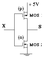
CMOS Complementary Metal Oxide Semiconductor
Abbreviation of complementary metal oxide semiconductor. Pronounced see-moss, CMOS is a widely
used type of semiconductor. CMOS semiconductors use both NMOS (negative polarity) and PMOS (positive polarity) circuits. Since only one of the circuit types is on at any given time, CMOS chips
require less power than chips using just one type of transistor. This makes them particularly attractive for use in battery-powered devices, such as portable computers. Personal computers also contain a small
amount of battery-powered CMOS memory to hold the date, time, and system setup parameters.
http://www.play-hookey.com/digital/electronics/cmos_gates.html
CTT Center Tap Terminated
The Center Tap Terminated, or CTT standard is a 3.3V memory bus standard sponsored by Fujitsu
(JESD8-4). This standard requires a Differential Amplifier input buffer and a Push-Pull output buffer.
ECL Emitter Coupled Logic
Emitter-Coupled Logic is based on the use of a multi-input differential amplifier to amplify and combine
the digital signals, and emitter followers to adjust the dc voltage levels. As a result, none of the transistors in the gate ever enter saturation, nor do they ever get turned completely off. The transistors
remain entirely within their active operating regions at all times. As a result, the transistors do not have a charge storage time to contend with, and can change states much more rapidly. Thus, the main
advantage of this type of logic gate is extremely high speed.
In operation, a logical ouput changes state by only 0.85 volt, from a low of -1.60 volts to a high of
-0.75 volt. The internal bias circuit supplies a fixed voltage of -1.175 volts to the bias transistor in the differential amplifier. If all inputs are at -1.6 volts (or tied to VEE), the input transistors will all be off,
and only the internal differential transistor will conduct current. This reduces the base voltage of the OR output transistor, lowering its output voltage to -1.60 volts. At the same time, no input transistors are
affecting the NOR output transistor's base, so its output rises to -0.75 volt. This is simply the emitter-base voltage, VBE, of the transistor itself. (All transistors are alike within the IC, and are
designed to have a VBE of 0.75 volt.)
http://www.play-hookey.com/digital/electronics/ecl_gates.html
GTL Gunning Transceiver Logic Terminated
The Gunning Transceiver Logic, or GTL standard is a high-speed bus standard (JESD8.3) invented by
Xerox. Xilinx has implemented the terminated variation for this standard. This standard requires a differential amplifier input buffer and a Open Drain output buffer.
GTL+ Gunning Transceiver Logic Plus
The Gunning Transceiver Logic Plus, or GTL+ standard is a high-speed bus standard (JESD8.3) first
used by the Pentium Pro processor.
HSTL High-Speed Transceiver Logic
The High-Speed Transceiver Logic, or HSTL standard is a general purpose high-speed, 1.5V bus
standard sponsored by IBM (EIA/JESD 8-6). It was developed for voltage scalable and technology independent I/O structures. The I/O structures required by this standard are; differential amplifier inputs
(with one input internally tied to a user-supplied input reference voltage for single ended inputs), and outputs using output power supply inputs (V CCO ) that may differ from those operating the device
itself. This standard has four variations or classes. SelectI/O devices support Class I, III, and IV. Single ended and differential input buffer specifications as well as various push-pull output driver specifications
are incorporated in this standard. HSTL devices accept a minimal differential input swing from 0.65 V to 0.85 V (nominally) with the outputs driving LVTTL levels. HSTL is ideally suited for driving an address
bus to two banks of memory. The HSTL input levels follow the JESD8-6 standard developed through the Joint Electronic Device Engineering Committee (JEDEC).
- HSTL compliance does not specify device supply voltages, making it a process-independent I/O standard. The lower voltage-level swing associated with this standard makes high-speed HSTL I/O solutions possible for any core voltage level device.
- A given circuit need not have all four classes of output drivers, but each circuit must have at least one of the four classes to claim HSTL output compliance.
- The HSTL nominal logic switching range is 0.0 V to 1.5 V, resulting in faster outputs with reduced power dissipation, and minimized EMI concerns.
- HSTL gives system designers enhanced flexibility in optimizing system performance with adjustable trip-point (V REF ) and output power supply voltage (V CCO ).
SSTL Stub Series Terminated Logic
SSTL-2 and SSTL-3 are low voltage signal swing interfaces for both single- and double date rate
synchronous DRAM. These standards support data rates of from 83MHz to 333MHz for memories made by Hyundai, NEC, Micron, Samsung, Siemens, and Toshiba. Applications include 3-D graphics
cards, plasma and LCD Displays, DTV interfaces, and set top boxes.
- SSTL3 Stub Series Terminated Logic for 3.3V
The Stub Series Terminated Logic for 3.3V, or SSTL3 standard is a general purpose 3.3V memory bus standard also sponsored by Hitachi and IBM (JESD8-8). This standard has two classes, I and II. SelectI/O devices support both classes for the SSTL3 standard. This standard requires a Differential Amplifier input buffer and an Push-Pull output buffer. - SSTL2 Stub Series Terminated Logic for 2.5V
The Stub Series Terminated Logic for 2.5V, or SSTL2 standard is a general purpose 2.5V memory bus standard sponsored by Hitachi and IBM (JESD8-9). This standard has two classes, I and II. SelectI/O devices support both classes for the SSTL2 standard. This standard requires a Differential Amplifier input buffer and an Push-Pull output buffer.
LVCMOS Low Voltage CMOS
Low-Voltage CMOS, 3.3 Volts CMOS
LVDS Low Voltage Differential Signal
LVDS, a point-to-point connection, is defined by two industry standards:
- ANSI/TIA/EIA-644 standard defines LVDS electrical specs including driver output and receiver input electrical characteristics. It does not cover functional specifications, protocols, or transmission medium characteristics since these are application dependent. The ANSI/TIA/EIA-644 is the more generic of the two standards, and is intended for multiple applications.
- IEEE 1596.3 SCI-LVDS standard is a subset of SCI (Scalable Coherent Interface). The SCI-LVDS standard defines electrical specifications for the physical layer interface of SCI. It is similar to the ANSI/TIA/EIA-644 standard but differs in the intended usage of the interface. It defines a lower voltage differential signal (as low as 250mV swing) that is compatible with CMOS, BiCMOS and GaAs circutry.
The IEEE committee created the SCI-LVDS standard for communication between SCI nodes (IEEE P1596.3-1995/D1.3 Standard for Low Voltage Differential Signals for Scalable Coherent Interface (SCI) Nov. 27, 1995).
Two different link subsets exist in SCI-LVDS standard: - General Purpose Link
- Reduced Range Link
|
In order to promoting a wider standard, no specific process technology, medium, or power supply voltages are defined by both standards. This means that LVDS can be implemented in CMOS, GaAs or other applicable technologies, migrate from 5V to 3.3V to sub-3V supplies, and transmit over PCB traces or cable serving a broad range of applications in many industry segments. Another voltage characteristic of LVDS is that the drivers and receivers do not depend on a specific power supply, such as 5V. LVDS has an easy migration path to lower supply voltages such as 3.3V and 2.5V, while still maintaining the same signaling levels and performance. In contrast, technologies such as ECL or PECL have a greater dependence on the supply voltage, which make it difficult to migrate systems utilizing these technologies to lower supply voltages.
|
http://www.national.com/appinfo/lvds/0,1798,100,00.html
LVPECL Low Voltage Positive Referenced Emitter Coupled Logic
Low-Voltage PECL - 3.3 Volts PECL
LVTTL Low Voltage Transistor-Transistor Logic
Low-Voltage TTL (LVTTL). As far as the minimum logic 1 level and the maximum logic 0 level are
concerned, LVTTL is identical to TTL: at an input, logic 0 is anything below 0.8 V and logic l is anything above 2.4 V. The difference between TTL and LVTTL stems from LVTTLs maximum logic 1 input
voltage, which generally cannot exceed the supply voltage by more than 0.3-1.0 V Thus, a 3.3 V LVTTL part has a maximum logic 1 input level that is below the typical logic 1 output level of most 5 V CMOS TTL parts.
PCI Peripheral Computer Interface
Peripheral Component Interconnect. Industry Standard CPU to Peripheral Bus interconnect intended
primarily for use in Personal Computers.See also on page Interfaces.
PECL Positive Referenced Emitter Coupled Logic
PECL originates from ECL but uses a positive power supply. The relatively small swing of the PECL
signal makes this logic suitable for high-speed serial and parallel data links. First developed by Motorola, the PECL standard has long since gained popularity with the rest of the electronics industry.
The PECL output structure consists of a differential pair that drives a pair of emitter followers. The output emitter followers should operate in the active region, with DC current flowing at all times. This
increases switching speeds and helps maintain fast turn-off times. The proper termination for a PECL output is 50... to (VCC2V). At this termination, both OUT+ and OUT- will typically be
(VCC...1.3V), resulting in a DC current flow of approximately 14mA. The PECL output impedance is low, typically on the order of (4-5) Ohms, which provides superior driving capability. When PECL
outputs drive a transmission line, this low output impedance, which generates a mismatch in back termination, can result in high frequency aberrations.
The PECL input structure is a current switching differential with high input impedance. In order to provide operating headroom, the common-mode voltage should be around (VCC-1.3V). The PECL
interface is suitable for both +5.0V and +3.3V power supplies. When the power supply is +3.3V, it is commonly referred to as low-voltage PECL (LVPECL).
Attention must be paid to power-supply de-coupling in order to keep the power-supply rail noise free. Also, the AC and DC requirements of the PECL outputs place additional constraints on termination networks.
RS-232
A single-ended serial transmission schematic is implemented by this standard. Maximum data rate can
now reach 120kbps. Cable length rates between 10 and 20 meters with a max load of 2500pF. Longer cable lengths and higher data rate require balanced connections lines.
RS-422
This standard allows only one differential way communication mode, using a twisted media pair. Max
data rate, not implied at max calbe length, is10Mbps. Max specified cable length is 1200m. Each driver can drive up to 10 receivers.
RS-423
An unbalanced line is used even if only one end of the transmission system is grounded in order to
prevent ground loops. Cable length rates between 30 (120kbps) and 1200 meters (3kbps).
RS-485
Thats primarily an upgrade of the RS-422 specified for multipoint bus to be constructed. This standard
meets and improves all the requirements of the RS-422 allowing, in addition, up to 32 drivers and 32 receivers to be connected to a single bus.
RSDS Reduced Swing Differential Standard
For the output section, FPGAs interface the imageprocessing to the panel-driving circuitry via LVDS or
the newly emerging RSDS standard. LVDS and RSDS are low-noise, low-power, low-amplitude differential signaling methods for sending high-speed (Gbps) data
transmission over copper wire. RSDS has a lower voltage swing
and output drive current than standard LVDS, resulting in
lower EMI and lower power consumption.
SLVS-400
The JEDEC standard SLVS-400 is a differential voltage-based signaling protocol. The nominal VOL of
0 (GND) and a nominal VOH of 400 mV. The driver impedance must be matched to the line and termination impedances requireing a nominal 800 mV power supply (VDDQ). SLVS defines the three
primitive drivers, receivers, and terminators.
www.jedec.org/download/search/jesd8-13.pdf
TTL Transistor-Transistor Logic
Transistor-Transistor Logic, a common type of digital circuit in which the output is derived from two
transistors. The first semiconductors using TTL were developed by Texas Instruments in 1965. The term is commonly used to describe any system based on digital circuitry.
http://www.play-hookey.com/digital/electronics/ttl_gates.html
VML Voltage-Mode Logic
VML drivers are implemented in CMOS and don't require external pull-up resistors because their
architecture uses NMOS and PMOS transistors to drive both, the falling and rising signal edges.
VML drivers are compatible with LVPECL when ac-coupled.
![]() (last update: September 2005)
(last update: September 2005)
[Home] [ASICs] [Selbstmanagement] [Inselmeer] [Spiele]
[Ich über mich] [Links] [SiteMap] [Disclaimer]